SMT PCB Assembly and Service
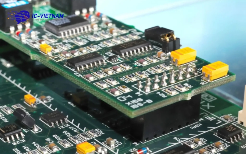
Surface Mount Technology (SMT) is a technique used for mounting electronic components onto the surface of printed circuit boards (PCBs). Unlike traditional methods where components are inserted into holes on the board, SMT allows for the components to be attached directly on the surface. SMT has revolutionized the way electronic assemblies are manufactured, allowing for advancements in technology and performance in modern electronic devices.
Introduction to SMT PCB Assembly
SMT is a method used for attaching electronic components directly to the surface of a Printed Circuit Board (PCB). It has significantly transformed the electronics industry by enabling the production of more compact, lightweight, and efficient electronic devices. SMT PCB Assembly is the process of creating PCBs by placing and soldering surface-mount components onto the PCB.

In contrast to traditional through-hole assembly, where components are mounted on the PCB by inserting their leads through holes, SMT components are soldered directly to the board using reflow soldering. This eliminates the need for drilling holes, allowing for a higher density of components and improved electrical performance.
The SMT Assembly Process
The SMT PCB Assembly process is a series of interconnected stages that ensure the precise placement and soldering of surface-mount components onto a PCB. Each step is crucial in maintaining the overall quality and performance of the final product. The main stages of the SMT process are as follows.
Step 1: Designing the PCB layout
The first stage in the SMT process is designing the PCB layout using specialized software. This involves determining the optimal placement of components, routing, and power distribution while adhering to industry standards and design rules. The PCB layout serves as a blueprint for the entire assembly process, guiding the placement of components and the routing of electrical connections.
Step 2: Preparing the SMT Stencil
In parallel with the PCB design, an SMT stencil is prepared to facilitate the accurate application of solder paste onto the PCB pads. The stencil is a thin sheet of metal (usually stainless steel) with precisely cut openings corresponding to the solder pads on the PCB. During the assembly process, the stencil is aligned with the PCB, and solder paste is spread across its surface using a squeegee.
Step 3: Placing the components
During the component placement stage, surface-mount components are placed on the PCB using specialized pick-and-place machines. These machines can accurately place thousands of components per hour, ensuring rapid assembly.

Step 4: Soldering
After component placement, the PCB is passed through a reflow oven, where the solder paste melts and forms a secure bond between the components and the PCB.
Step 5: Inspection and Testing
The assembled PCB is subjected to various inspection and testing processes, such as Automated Optical Inspection (AOI) and X-ray inspection, to ensure the quality and functionality of the board. Quality control is an essential aspect of the SMT PCB Assembly process, ensuring that the final product meets the desired performance and reliability standards. Various inspection and testing methods are employed throughout the assembly process, including:
Step 6: Automated Optical Inspection (AOI)
AOI is a non-contact inspection method that uses high-resolution cameras and advanced image processing algorithms to detect defects in the assembled PCB, such as missing, misaligned, or damaged components, and soldering issues like insufficient solder or bridging.
Step 6: X-ray Inspection
This technique is used to inspect the solder joints of components that are not visible to the naked eye, such as those in Ball Grid Array (BGA) packages. X-ray inspection allows for the detection of soldering defects, such as voids or insufficient solder, ensuring the reliability of the assembled PCB.
Step 7: In-circuit Testing (ICT) and Functional Testing
These tests are performed on the fully assembled PCB to verify its electrical functionality and compliance with design specifications. ICT involves testing individual components and connections, while functional testing evaluates the overall performance of the PCB in its intended application.
SMT Equipments for PCB Assembly
The SMT machine plays a critical role in automating the assembly process, ensuring high accuracy, speed, and consistency.
SMT Stencil Printers
The SMT Stencil Printer, or the SMT screen printing machine, is the first step in the SMT production line, printing solder paste and glue to the PCB circuit board in preparation for the later patch process.
Surface Mount System
The Surface Mount System is the most technologically advanced manufacturing equipment in the SMT production line, capable of accurately and non-destructively mounting components to the PCB circuit board in the required place. There are numerous benchmarks for measuring the function of a mounter, the most essential of which are mounting speed, mounting accuracy, PCB standard, and mounting scale. The purpose of the placement machine serves as the primary benchmark for the resolution of the entire SMT production line.
There are numerous varieties of mounters for different applications and situations, including multi-function mounters, small mounters, high-speed mounters, LED special mounters, and so on.

Pick-and-Place Machines
These machines pick up surface-mount components from their storage containers (usually tapes or reels) using a vacuum nozzle, align them with the PCB pads, and place them on the solder paste. Advanced pick-and-place machines can handle a wide range of component sizes and types and can place thousands of components per hour.
SPI Machine
The SPI machine can check the solder paste for faults. It is used to check the thickness, area, and volume distribution of the solder paste printed on the PCBs, ensuring that everything meets standards before proceeding to assembly.
Reflow Oven
After the components have been placed on the PCB, the board is passed through a reflow oven, where the solder paste is heated to its melting point, allowing it to flow and form a secure bond between the components and the PCB. The reflow oven’s temperature profile is carefully controlled to ensure consistent soldering without damaging the components or the PCB.

Curing Oven Machine

After the components have been placed on the PCB, the board is passed through a reflow oven, where the solder paste is heated to its melting point, allowing it to flow and form a secure bond between the components and the PCB. The reflow oven’s temperature profile is carefully controlled to ensure consistent soldering without damaging the components or the PCB.
AOI Machine
The AOI machine is frequently utilized before and following the reflow process. It is used to detect component placement failures before to soldering in pre-solder inspection and soldering mistakes in post-solder inspection.
SMT Components and Packaging
SMT components come in various types, sizes, and packaging styles, enabling the assembly of a wide range of electronic devices. This section provides an overview of the most common SMT components and packaging styles used in the electronics industry.
Passive Components: Passive components are essential building blocks in electronic circuits, and they do not produce energy or amplify signals. The most common passive SMT components include:
Resistors: SMT resistors are used to limit current flow, divide voltage, and set signal levels in electronic circuits. They come in various sizes, such as 0603, 0805, and 1206, which refer to their dimensions in hundredths of an inch (e.g., 0603 resistors measure 0.06 x 0.03 inches).
Inductors: Inductors are passive components that store energy in their magnetic field and oppose changes in current. They are commonly used in filters, transformers, and power supply circuits.

Active Components: Active components can control the flow of current and amplify signals. They play a crucial role in electronic devices and come in various packaging styles. The most common active SMT components include:
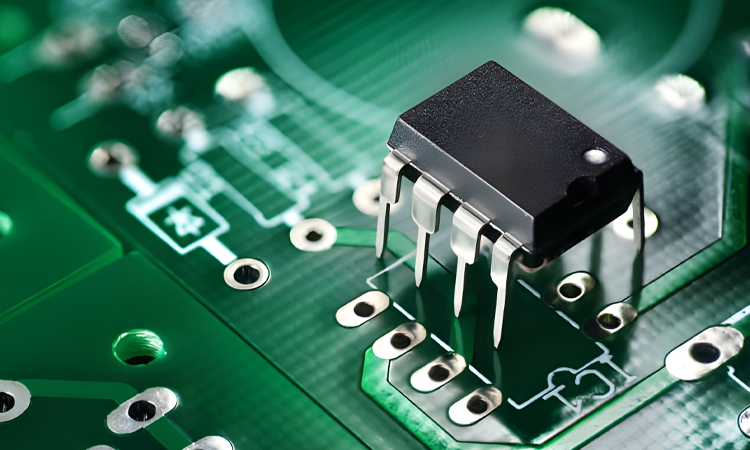
Integrated Circuits (ICs): ICs are compact electronic devices that contain multiple transistors, resistors, capacitors, and other components on a single semiconductor chip. SMT ICs are available in various package types, including Quad Flat No-Lead (QFN), Small Outline Integrated Circuit (SOIC), and Ball Grid Array (BGA).
Component Packaging Styles: SMT components come in a variety of package types to meet the needs of diverse applications and assembly requirements.
Some of the most common SMT packaging styles include:
Chip packages: Chip components, such as resistors, capacitors, and inductors, are the simplest SMT packages. They consist of a rectangular or square body with metal terminations on either end.
Leadless packages: Leadless components, such as QFN and DFN ICs, have metal pads on their bottom surface for soldering directly onto the PCB. These packages offer a compact footprint and improve thermal performance.
Lead frame packages: Lead frame components, such as SOIC and SOT transistors, have leads that extend from the body and are soldered onto the PCB. These packages provide a balance between ease of assembly and component size.
Ball Grid Array (BGA) packages: BGA components have an array of solder balls on their bottom surface for soldering onto the PCB. This packaging style allows for a high density of connections in a small footprint, making it suitable for advanced ICs with numerous pins.
Advantages of SMT PCB Assembly
SMT PCB Assembly offers numerous advantages over traditional through-hole assembly, including smaller and lighter devices, improved performance due to reduced parasitic effects, cost-effectiveness, and faster assembly times. As a result, SMT has become the dominant assembly method for modern electronic devices, ranging from smartphones and laptops to advanced automotive and aerospace systems.
The key benefits of SMT PCB Assembly include space efficiency, improved performance, cost-effectiveness, and faster assembly times. These advantages are discussed in detail below:
Space Efficiency: One of the most significant advantages of SMT PCB Assembly is the efficient use of space on the PCB. SMT components are smaller and can be placed directly onto the surface of the board, eliminating the need for drilling holes for component leads. This allows for a higher density of components and more complex circuit designs within a smaller area, contributing to the miniaturization of electronic devices.
Improved Performance: SMT PCB Assembly offers better electrical performance compared to through-hole assembly. The shorter electrical paths between components result in reduced parasitic effects, such as capacitance and inductance, leading to faster signal propagation and improved overall performance. Additionally, the lower mass of SMT components makes them less susceptible to mechanical vibrations, further enhancing the reliability of the assembled PCB.
Cost-Effectiveness: SMT PCB Assembly is more cost-effective than through-hole assembly due to several factors. First, the smaller size of SMT components typically results in lower material costs. Second, the elimination of drilling holes for components leads to reduced manufacturing time and costs. Finally, the automation of the SMT process using advanced pick-and-place machines and reflow ovens allows for higher production rates and reduced labor costs, contributing to a more cost-effective assembly process.
Faster Assembly Process: The SMT PCB Assembly process is faster than traditional through-hole assembly, primarily due to the high level of automation involved. With the use of advanced pick-and-place machines and reflow ovens, PCB manufacturers can achieve rapid assembly times, enabling them to meet tight production schedules and deliver products more quickly to the market.
Disadvantages of SMT PCB Assembly
Expensive Equipment: Most SMT types of equipment, including reflow ovens, selecting machines, solder paste screen printers, and even hot air SMD rework stations, are pricey. As a result, an SMT PCB assembly line demands a large investment.
Difficult Inspection: Since most SMD components are tiny and have many solder joints. BGA packages include solder balls and joints underneath the component, making inspection difficult.
Expensive Small-volume Production: Also, making SMT PCB Prototype or small batch production is expensive. Certain technological complications demand extensive skill and training.



































































 Chat
Chat


